Lesson
Introduction to FPGA
Introduction to Electronic Circuit
Electronic circuits in general can be divided into 2 categories: analog circuits and digital circuits.

Analogue circuit
An analog circuit processes and manipulates continuous electronic signals using components such as resistors, capacitors, inductors, and transistors.
Example: Power modules, Amplifier, Radio Frequency Application Circuit
Digital circuit
A digital circuit processes discrete signals represented by binary digits (0s and 1s)
It uses components such as logic gates, flip-flops, and registers, which are also mainly constructed by transistors.
Example: Microprocessor, Digital Signal Processor, Graphical Processing Unit(GPU), Programmable Logic Device
In this course, we will discuss mainly digital circuits.
Common Circuit vs Integrated Circuit
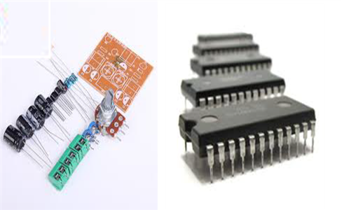
Common circuit is built using discrete electronic components like resistors, capacitors, transistors, and other components. These components are individually assembled and interconnected on a PCB (Printed Circuit Board) or breadboard.
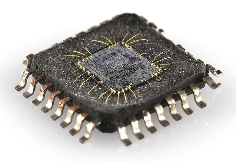
Integrated circuit or Chip is a single semiconductor device that integrates multiple electronic components, such as transistors, resistors, capacitors, and interconnections circuits. ICs are fabricated using various semiconductor manufacturing processes, such as photolithography and chemical vapor deposition.
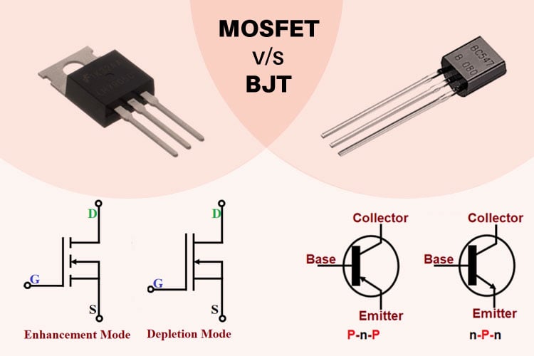
Foundation of Integrated Circuit - Transistor
Transistors are semiconductor devices used to amplify or switch electronic signals and electrical power. There are two commonly used transistors: Bipolar Junction Transistor(BJT) and Metal-Oxide-Semiconductor Field-Effect Transistor(MOSFET).
Example: MOSFET and BJT IC
Imagine you are going to build a simple switch circuit. Surely you can use a mechanical switch. However, physical presses are required for activating or deactivating the circuit. What if pressing is not allowed or compatible in your application scenario (e.g. the switch circuit implemented underground)?
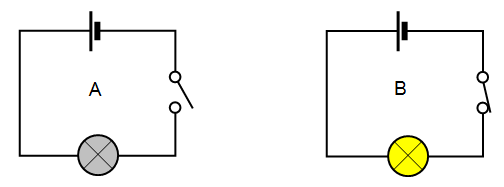 By using a transistor, we can create an electrical signal-controlled "switch" circuit. The following example is done by an NPN BJT.
Example: An opened "switch" implemented by NPN BJT

Example: A closed "switch" implemented by NPN BJT

By using a transistor, we can build an amplifier circuit, which is the basis of Anlogue Integrated Circuit , or a switch circuit, which is the basis of Digital Integrated Circuit.
We use multiple transistors to form different kinds of digital logic gates, which are the basic building blocks from all digital circuits and microprocessor-based systems.
Introduction to Digital Circuit
Logic Gate
Digital Circuit manipulate electronic input and output signal using logic gates. Engineers will utilize different combinations of logic gates can fullfil certain tasks.
The basic structure of a logic gate are 2 input signals, 1 output signals and the logic gate itself.

Example: An AND gate circuit implemented by 2 NPN BJT

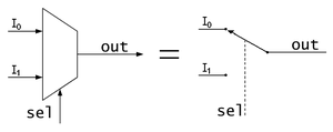
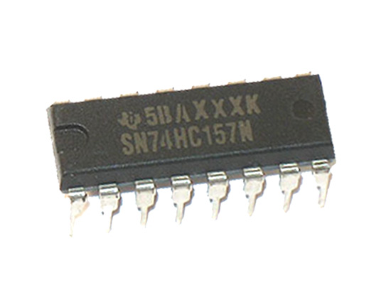
Multiplexer (MUX)
Multiplexer allow engineers to use input control signals switch the output signal between different input signals, acting as an mechanical dip switch.
 Example: A MUX IC
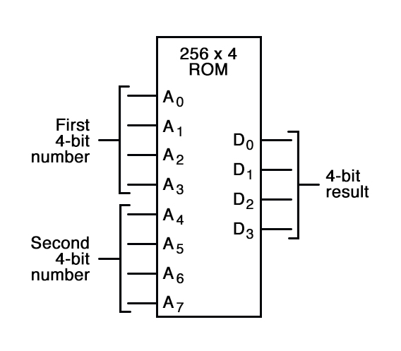
Lookup Table (LUT)
Lookup Table map all the possible combination of input signal to a programmed-set of output signals. Lookup Table is commonly built by Read-Only Memory(ROM) device, where a logic gates combination circuit will be mapped to the lookup table in the ROM.

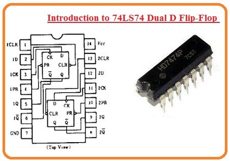
Flip-Flop
While Logic Gates, MUXs, Lookup Tables can handle most of the decision-making tasks, they lack the ability to store the input signal as data ** in the form of ** memory.
Flip-Flop is a basic building block used to construct more complex digital systems, such as counters, registers, and block memory.
Example: A commonly used Data Flip-Flop
Example: A Data Flip-Flop IC
Development of Integrated Circuit
The development of integrated circuits and chips can be easily illustrated by the Scale of Integration, which distinguishes how many transistors can be fitted into a defined surface area on a semiconductor material.
| Scale of Integration | Name | Year | Transistor count | Logic gates number | Example |
|---|---|---|---|---|---|
| SSI | small-scale integration | 1964 | 1 to 10 | 1 to 12 | Flip-Flops |
| MSI | medium-scale integration | 1968 | 10 to 500 | 13 to 99 | Counters |
| LSI | large-scale integration | 1971 | 500 to 20 000 | 100 to 9999 | Intel 4004(First mircroprocessor) |
| VLSI | very large-scale integration | 1980 | 20 000 to 1 000 000 | 10 000 to 99 999 | System on Chip(SoC) |
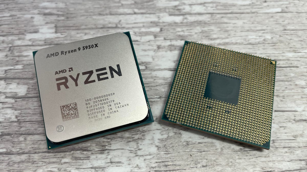
| ULSI | ultra-large-scale integration | 1984 | 1 000 000 and more | 100 000 and more | AMD Ryzen 9 |
Digital IC in nutshell: Parallel vs Sequential Processing
A video to emulated how CPU and GPU work in a fun way! Adam and Jamie Paint the Mona Lisa in 80 Milliseconds! (HD) - YouTube
Programmable Logic Device(PLD)
Programmable Logic Devices are digital ICs with numerous digital logic gates built in. Engineers and developers can design and program the digital logic inside it using Hardware Description Language(HDL).
Read-Only Memory(ROM)
Before the digital logic array IC, engineers tried to use ROM to represent combinational logic circuits as Lookup Table. Electrically Erasable Programmable ROM(EEPROM) was commonly used. However, using a memory device to represent digital logic circuits is slow and cost-ineffective. Thus, an array circuit built by numerous interconnected logic gates is widely used for PLD instead.
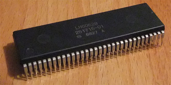
Example: A EEPROM IC
Programmable Logic Array(PLA) and Programmable Array Logic(PAL)
Both PLA and PAL consist of an AND Array and an OR Array.
Difference is:
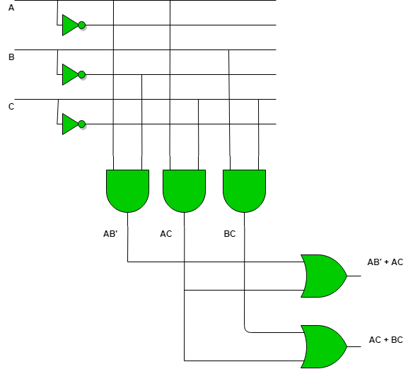
- In a PAL, the AND array is fixed, but the OR array is programmable.
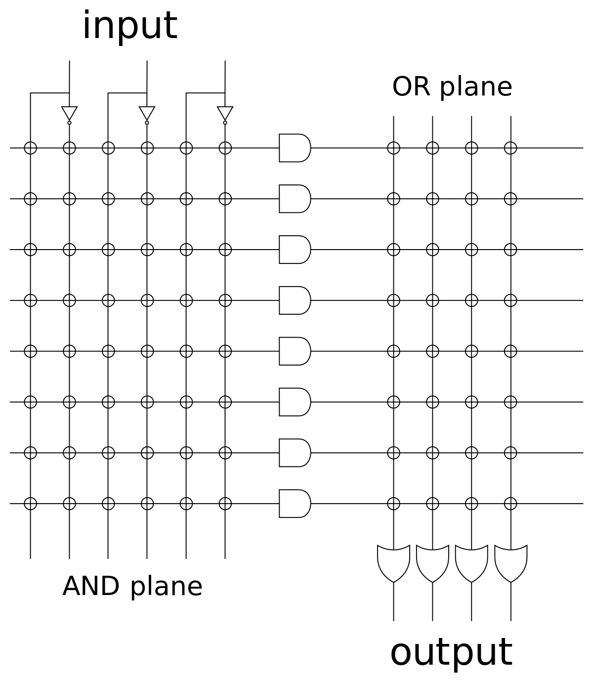
- In a PLA, both the AND and OR arrays are programmable.
PAL or PLA can be programmed by anti-fuse technology(irreversible) or EEPROM.
Example: A PLA IC
Field Programmable Gate Array (FPGA)
![FPGA Design, Architecture and Applications (Updated) [2024]](https://www.logic-fruit.com/wp-content/uploads/2021/12/FPGA-Graphics-1.jpg.webp)
Based on PAL and PLA, FPGA is developed to fulfill more complex and large-scale digital circuit applications. The key feature of FPGA is "field", which means the digital circuit design can be reprogrammed outside the factory, which gives us greater flexibility and agility in utilizing it.
Example: Xilinx Artix-7 FPGA development board

Structure of a FPGA
- Logic Blocks:
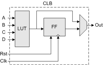
- FPGAs consist of a large number of configurable logic blocks (CLBs) that can be interconnected to implement various logic functions. Each CLB typically contains Lookup Tables(LUTs), flip-flops, and multiplexers.
- Interconnect:
- The interconnect structure of an FPGA comprises a network of programmable routing resources that allow signals to be routed between the CLBs. This interconnect provides flexibility in establishing connections between different logic blocks based on the desired circuit configuration.
- Configuration Memory:
- FPGAs use configuration memory to store the programming information that determines the functionality of the device. This memory is used to configure the interconnect resources, logic blocks, and other functional elements within the FPGA.
- I/O Blocks:
- Input/output blocks (IOBs) provide the interface between the internal logic of the FPGA and the external world. These blocks allow the FPGA to communicate with external devices, such as sensors, memory, or other integrated circuits.
- Clock Distribution:
- FPGAs have dedicated resources for distributing clock signals throughout the device. These resources help in ensuring synchronous operation of the internal logic elements and facilitate the implementation of complex synchronous designs.
- Embedded RAM and DSP Blocks:
- Some FPGAs include embedded memory blocks and digital signal processing (DSP) blocks to provide additional functionality for specific applications that require memory or digital signal processing capabilities.
Application Specific Integrated Circuit(ASIC)
Unlike PLA and FPGA that can be programmed to meet a variety of use case requirements after manufacturing, ASIC designs are tailored early in the design process to address specific needs. ASIC is expensive, and consumes much time to develop and manufacture. Thus, it are only used in very specific and dedicated task in an electronic system.
It is very common for chip engineers to use FPGA to test and evaluate an ASIC design before manufacturing the acutal ASIC.
Example: Targeted AMD ASIC dedicated for Interactive Streaming

General Purpose Processor
Central Processing Unit (CPU), Microcontroller Unit (MCU), and Microprocessor are the common general-purpose processors,
Example: AMD Ryzen 9 CPU
Unlike PLDs, a General purpose processor is designed to run a large variety of general instructions to cater to the most number of scenarios as possible. Thus, many logic gates are compiled together to form defined function blocks, such as Control Unit(CU), Arithmetic Logic Unit(ALU), Registers.
Working Process of General Purpose Processor
1. Fetch
-
The Control Unit (CU) retrieves ("fetches") the next instruction to be executed from the main memory (RAM) and places it into the Instruction Register (IR).
-
The address of the instruction is stored in the Program Counter (PC), which is then incremented to point to the next instruction.
2. Decode
-
The fetched instruction is sent to the Instruction Decoder within the Control Unit.
-
The Control Unit interprets the instruction to understand what operation is to be performed and which resources are required.
3. Execute
-
The decoded instruction is sent to the appropriate part of the CPU. For instance, if it’s an arithmetic operation, it will be sent to the ALU.
-
The required data is fetched from the registers or memory.
-
The ALU performs the required operation (addition, subtraction, logical operations, overflow detection, etc...).
-
The result of the operation is stored back in a register or memory.
4. Write Back
-
The result of the execution stage is written back to the appropriate place, such as a register or a memory location.
-
This step updates the status registers and flags (like zero, carry, overflow) based on the result of the operation.
Comparison between different Digital IC
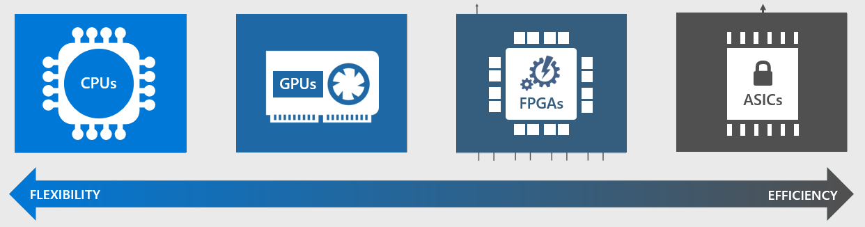
All the abovementioned digital IC can be compared in 2 parameters: Flexibility and Efficency.
As mentioned before, general purpose processor's architecture is designed to run a large variety of general instructions to cater to the most number of scenarios as possible. However, many steps are required for running a task in a general-purpose processor, resulting in an efficiency bottleneck.
FPGA and ASIC on the other hand, can be designed for specific repetitive applications or task in a very efficient way.
Multiprocessor System-on-Chip(MPSoC)
Multiprocessor System-on-Chip is a technology to integrate general processor(CPU, GPU), FPGA, and DSPs into one system chip. With MPSoC, engineers and developers can allow different processors to cooperate with each other. General processes can assign repetitive tasks to a dedicated processor, such as FPGA and GPU, such that they can accelerate the task. Thus, the whole system can work in a faster speed and greater efficiency.
Key Application of MPSoC:
AI and Machine Learning, Automotive, Telecommunication
Zynq® UltraScale+™ MPSoC and Ultra96
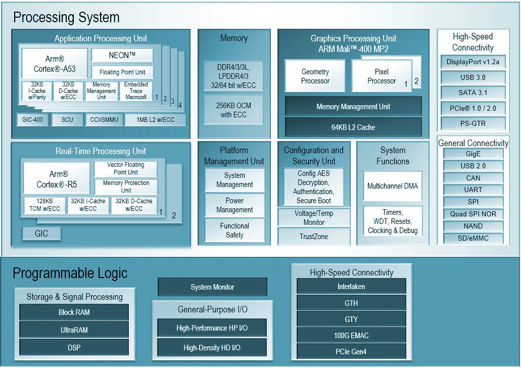
Developed by AMD Xilinx, Zynq® UltraScale+™ MPSoC combines the capabilities of a traditional FPGA in the name of "Programmable Logic" with a high-performance processing system, making it a powerful and versatile platform for a wide range of applications.
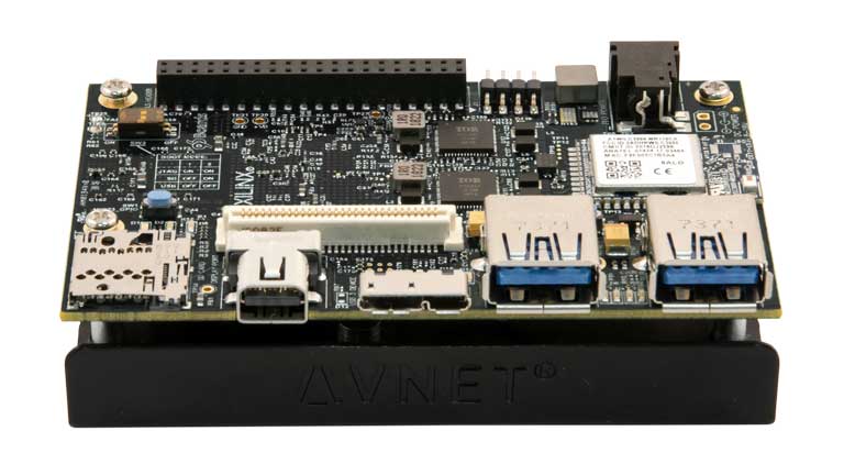
Example: Zynq® UltraScale+™ MPSoC used in our main course hardware: Avnet Ultra96-V2 development board
AMD Xilinx Vivado
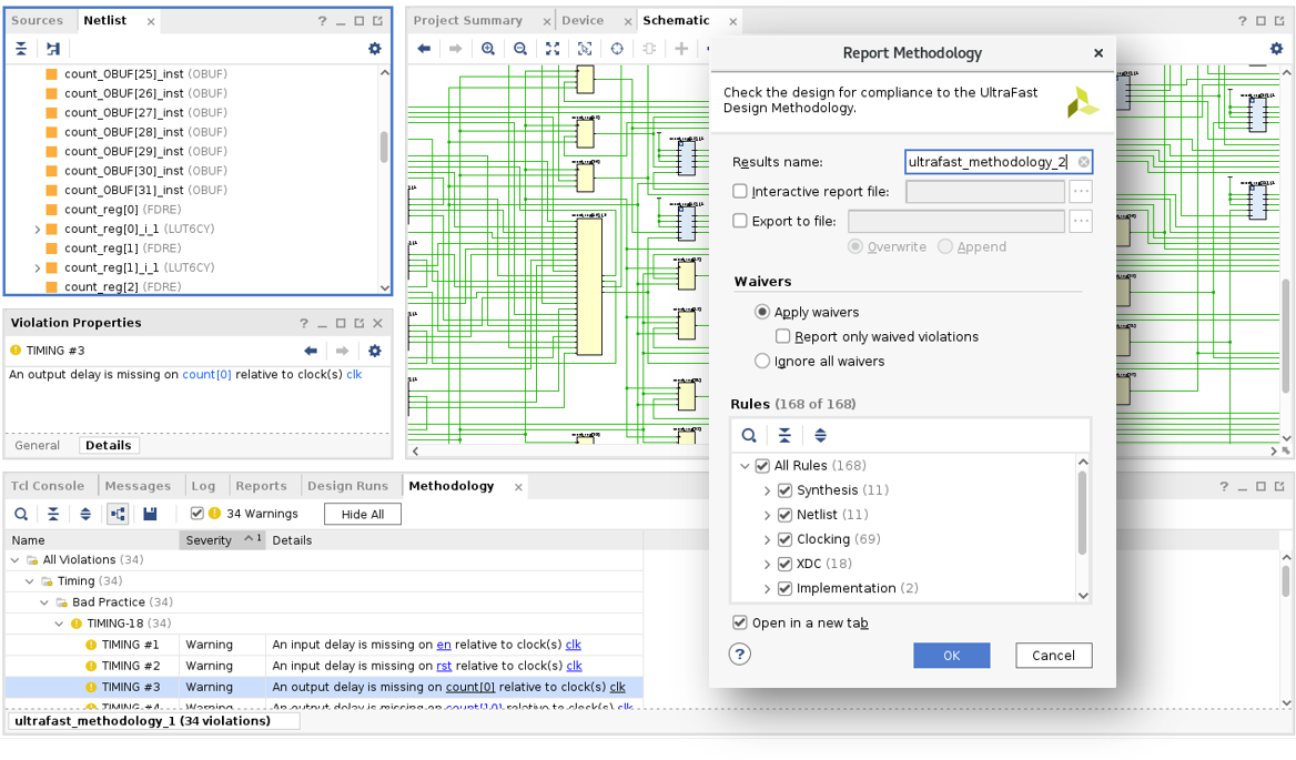
To design, implement, and verify digital logic circuits for the Programmable Logic in Zynq® UltraScale+™ MPSoC or Xilinx FPGA, Xilinx Vivado design suite is primarily used.
Key Features and capabilities of the AMD Vivado
-
Integrated Design Environment (IDE):
-
High-Level Synthesis (HLS)
-
IP Integrator
-
Implementation and Optimization
-
Verification and Debugging
PYNQ
PYNQ stands for Python Productivity for Zynq. It is an open-source project that enables programming MPSoCs with Python.
A great tool for prototyping and exploring FPGA designs using a high-level language like Python.
Initializing PYNQ on Ultra96
Follow the documentation to connect Ultra96 to your computer:
https://ultra96-pynq.readthedocs.io/en/latest/getting_started.html
In your browser, connect to http://192.168.3.1/. Enter Login password: xilinx to start using Jupyter Notebook.
Using Juypter Notebook in PYNQ
Juypter Notebook is used as the GUI IDE for PYNQ. Juypter Notebook support running Python notebook and Linux terminal.

Open and Run a Displayport example notebook
-
Connect MiniDisplayport to DP-to-HDMI converter, HDMI cable, and HDMI Video Capture card
-
Connect HDMI Video Capture card to your computer's USB port
-
Connect the Webcam to Ultra96's USB port
-
Open "common" folder
-
In the "common" folder, open "display_port_introduction.ipynb" notebook

- Make sure you connect everything properly and open the "Camera" application in your computer.

- Run the whole notebook to display camera output to your computer

Using Linux Terminal in Juypter Notebook in PYNQ
Go back to the Homepage. Initialize a new terminal by pressing New > Terminal.


Common Linux Command
-
ls: Lists the contents of a directory. -
cd: Changes the current working directory. -
mkdir: Creates a new directory. -
rm: Removes (deletes) files or directories. -
cp: Copies files or directories. -
mv: Moves or renames files or directories. -
cat: Displays the contents of a file. -
nano: A text editor for editing files. -
ssh: Connects to a remote machine via Secure Shell (SSH). -
chmod: Changes the permissions of a file or directory. -
sudo: Executes a command with superuser (administrative) privileges. -
grep: Searches for a pattern in a file or output. -
top: Displays the running processes and their system resource usage. -
apt-get: The package manager for Debian-based Linux distributions (e.g., Ubuntu). -
systemctl: Manages system services (start, stop, enable, disable).