Lesson
Introduction to Overlay in Xilinx MPSoC design
FPGA design flow with Xilinx Vivado
To design, implement, and verify digital logic circuits for the Programmable Logic in Zynq® UltraScale+™ MPSoC or Xilinx FPGA, Xilinx Vivado design suite is primarily used. Let's take a deeper look in the process of developing and implementing a digital circuit on an FPGA device using Xilinx Vivado.
1.1 Digital circuit design with Hardware Descripton Language(HDL)
Other than building the digital circuit from scratch using wires and ICs, we use Hardware Descripton Language(HDL) to aid us to design digital circuit in computer tools like Vivado. Common HDL are Verilog and VHDL.
First of all, HDLs are NOT programming language like C++ or Python. C++ or Python are instructions , running in the CPU in the way that we discussed before. While HDLs essentially describe the behaviour and connection between different digital circuit hardwares.
Example: Logic gates combination in Verilog and in acutal circuit diagram
	(input a,b,c,d,e,
	output z)

	assign z =((a&b)|(c^d)&~e);

1.2 Digital circuit design with Intellect Property(IP) Blocks and Block Diagram
Another more efficient and stable way to perform digital circuit design is to use Intellect Property(IP) Blocks. IP Blocks are pre-designed and pre-verified digital circuit components written in HDLs that can be integrated into larger IC design.
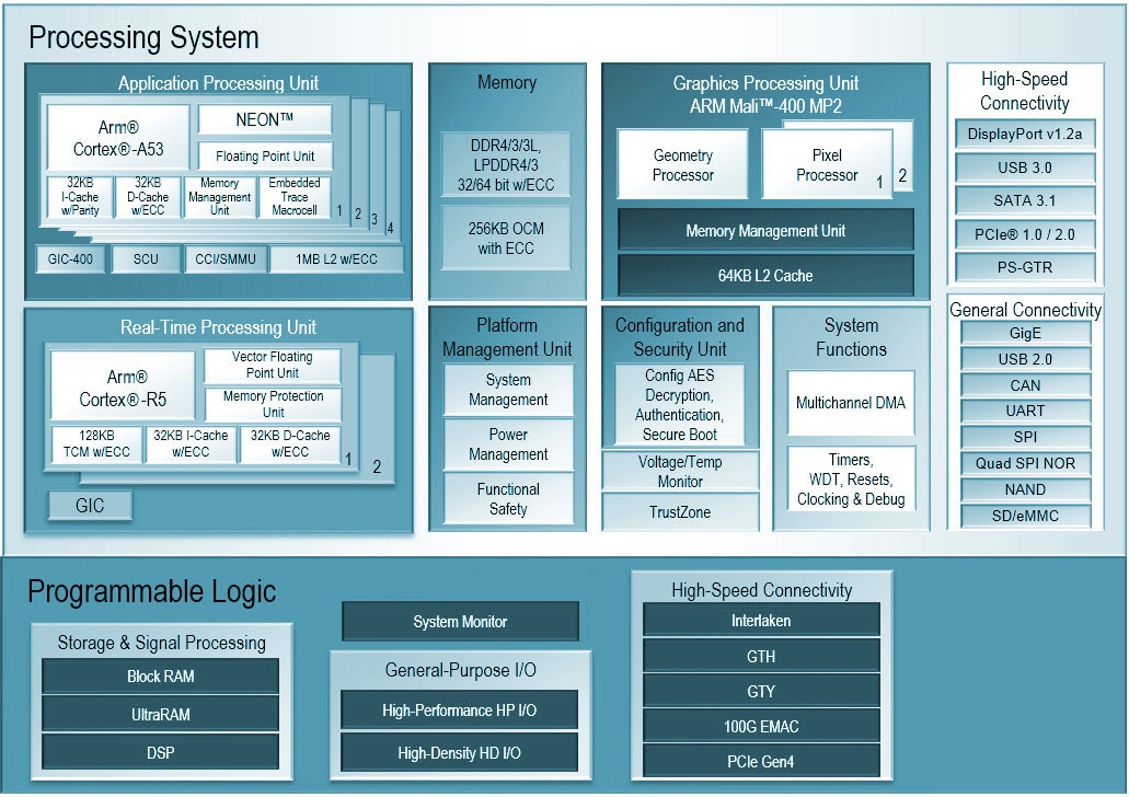
Example: Block diagram of the Base overlay in Ultra96. Here we can see they reuse 2 identical AXI UART Block.

2. Synthesis
After completing the circuit design with HDLs, synethsis need to be done to convert the code into a netlist, which is a list of logical components (gates, flip-flops, etc.) and their interconnections.
3. Simulation and Verification
Engineers can use Verilog to simulate the circuit based on the result of sythesis, to ensure the design meets the required specifications and behaves as expected. Engineers will review the circuit functionality based on the timing diagrams of input and output signals.
Or, engineers can use SystemVerilog to create testbench to test the circuit with software programs.
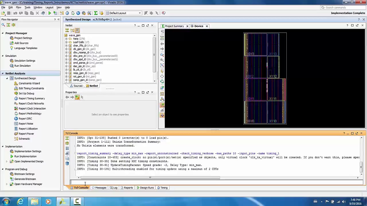
Example: Timing diagram in Verilog from a Simulation
4. Implementation
One of the strength of designing digital circuit with HDLs is that the design can basically be applied to any FPGA device.
In Vivado, implementation tools allow engineers to place the synthesized netlist is placed on the specific FPGA's physical resources, such as logic blocks, memory, and I/O pins. Routing will be done to connects the placed components using the available interconnect resources on the FPGA.
Then, timing analysis can be performed to make sure the whole circuit design is synchronous.
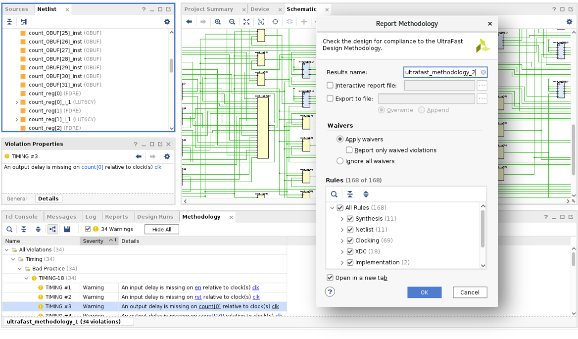
Example: Implementation Report in Vivado
5. Generation Bitstream
After Implementation, the placed and routed circuit design is translated into a configuration bitstream, which is a binary file that can be used to program the configuration block inside FPGA.
Although we won't go through the FPGA design flow step-by-step in the lesson, you can refer to the "Vivado" page to suppliment your understanding.
Overlay in Ultra96 - GPIO
 In last lesson we introduced the development and trend of digital IC. MPSoC is one of the solution to combine the flexibilty of General Processor System(PS) and processing power of Programmable Logic(PL) in one system.
In Ultra96, we can use PYNQ, which allow us to run Python code on the PS using Juypter Notebook in a simple way.
Base Overlay
Overlay is a python interface in PYNQ to allow PS interpret, communicate and control the digital circuit in PL using Python code and Jupyter Notebook.
Example: Block diagram of the Base overlay in Ultra96, provided with 2 AXI UART Block.
Loading the overlay
You can try to open the "creating_Ultra96_overlays.ipynb" and run the first 2 blocks of code in the notebook to load the overlay.

By loading the overlay, the Python code will instruct PS to use the defined bitstream to program the PL
PS GPIO
GPIO (General-Purpose Input/Output) refers to the digital pins on an electronic device, such as a microcontroller or FPGA, that can be programmed to function as either inputs or outputs. GPIO pins provide a flexible way to interface the device with various external components and sensors.
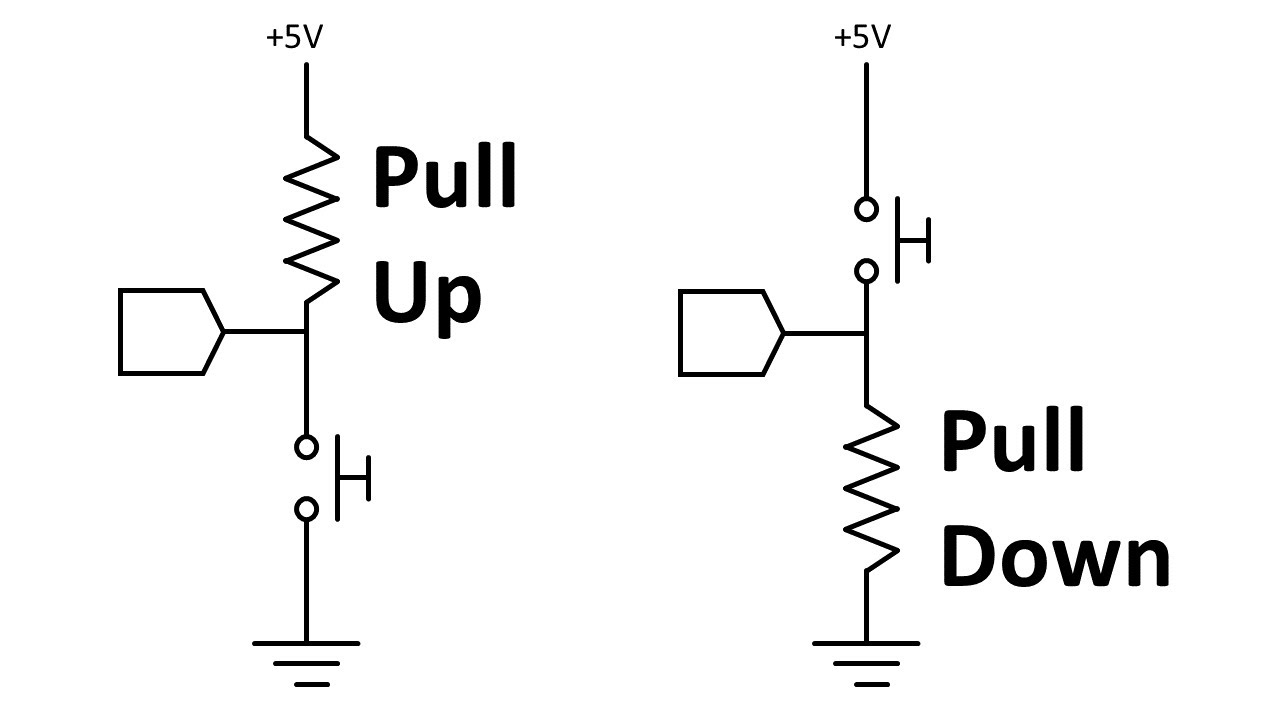
GPIO pins often need to be accompanied by pull-up or pull-down resistors, which can be used to define a default logic level (HIGH or LOW) when the pin is not driven by an external source.
Example: Pull-up/Pull-down resistor for GPIO
To use GPIO and Ultra96v2, the first thing to note is that there are two types of GPIO. PS GPIO and PL GPIO.
-
PS GPIO runs on the Processing system (PS) and thus is accessable without an overlay. PYNQ provides some drivers such that you can use python code to drive the PS GPIO.
-
PL GPIO runs on the Programmable Logic (PL) and thus would require an overlay to utilize. Instructions to build the overlay can be found on the Vivado tab.
To utilize PS GPIO on PYNQ, it is similar to how you would run it on a linux embedded platform like Raspberry Pi.
Installing Ultra96 breakout board
The provided Ultra96 breakout board have both PL and PS 2.54mm jumper pinouts avaliable for development uses.
CAUTION: Make sure your install it CORRECTLY(matching the pins) such that you won't damage Ultra96 or the breakout board.

PS GPIO Library
Open a new folder "Exercise". From here, open a new Notebook "PS GPIO".
First, import the GPIO and time libraries so that you can add a delay before turning on and off the GPIO such that you can manipulate external electronic devices.
from pynq import  GPIO

import time
Then get the base number of the GPIO using
gpio_base = GPIO.get_gpio_base()
By calling the base, we can easaily define what pins we would like to use later on based on their number instead of having to calculate the number which maps to the coressponding pin.
Now we have to decide which pin number to use as well as the direction of the pin (whether it is an input or output). This can be done using the following code
gpio1 = GPIO(gpio_base+36, 'out') # write an output pin at pin 36

gpio2 = GPIO(gpio_base+37, 'in')

#write an input pin at pin 37
Once this is done we can decide to read or write on the coresponding pin.
gpio1.write(1)

# writes a high signal out of 1.8V

gpio1.write(0)

#writes a low signal out of 0V

gpio2.read()

#reads the voltage level at the pin when run if 1.8V will return 1 else if 0V will return 0.

#Has a threshold value for 1 and 0
Note you cannot write on a read pin or read on a write pin. You have to release the pin using the below before changing the direction of the pin
gpio1.release()
gpio2.release()

# gpio1 should be replaced with the variable you assigned your pin name
LED Example
Reminder: LED Polarity

- Connect the cathode of the LED to breadboard row 1, anode to row 2. Connect a resistor to breadboard row 2 and row 6.

- From the breakout board, connect IO36 pin to the same row of cathode of the LED using jumper wire. Connect GND pin to the row 6 using jumper wire.
 3. Toggle the LED using the abovemention Python code.
Generating PWM signal with PS GPIO Library
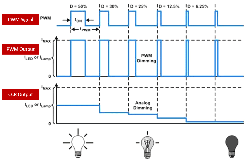 PWM (Pulse Width Modulation) is a technique used to control the amount of power delivered to an electrical device by alternating the duty cycle of a square wave signal. It is a widely used method in various electronic applications, including motor control, lighting, and power management.
The PWM pulse is square wave signal, which is characterized by a period (T) and a pulse width (t). From this we can deduce the frequency of the PWM signal using the following formula:
$$ Frequency = 1 / Period $$
The duty cycle is the ratio of the pulse width (t) to the period (T), expressed as a percentage. The duty cycle determines the proportion of time the signal is in the "high" state compared to the "low" state.
$$ Duty Cycle = (t / T) × 100% $$
Now that PS GPIO has been covered, use them to create a PWM signal, an easy method would be to use time.sleep() and a while loop. For example
while(True):

gpio1.write(1)

time.sleep(0.1)

gpio1.write(0)

time.sleep(0.9)

# provides a pulse every 1 second

# 10% duty cycle with 1Hz

# You can adjust the ratio of time.sleep() to increase the duty cycle and the reduce the time.sleep() duration to increase its frequency based on what you would like it to be
For more details on which Pins are in the PS GPIO please check the official documentation. It should be the MIO pins 36,37,39,40,44,45.
In class Hardware exercise
By the abovementioned PS GPIO example, create a hardware prototypes with the following features using the provided material and your electronic+software knowledge:
Task: LED Blink
- Using the light sensor as GPIO input
- GPIO output to LED
- When the light sensor doesn't sense anything, the LED blinks in this pattern: 1 second HIGH -> 1 second LOW ->repeat
- When the light sensor sense something, the LED blinks quicky three times in one second and then off for another second, repeat